

Please select your location and preferred language where available.
創新技術,為更高容量鋪路

前端製程技術
CBA 技術
專訪
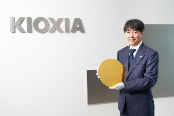
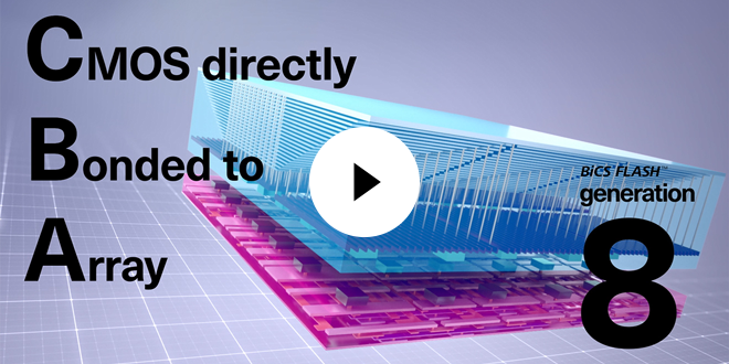
High-density 3D flash memory using high-precision wafer bonding brings new value to storage
In recent years, flash memory manufacturers have focused primarily on developing technologies to increase the number of layers of memory cells and increase memory density. Each time a new generation of flash memory is released, the number of layers increases with some products boasting more than 200 layers. However, as Atsushi Inoue, Vice President of Memory Division at KIOXIA, explained, "Increasing the layers of memory cells is only one way of increasing capacity and memory density, and we are not exclusively preoccupied with the number of layers."
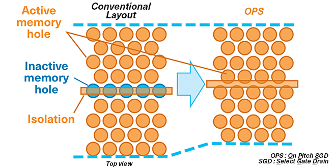
OPS 技術
後端製程組裝技術
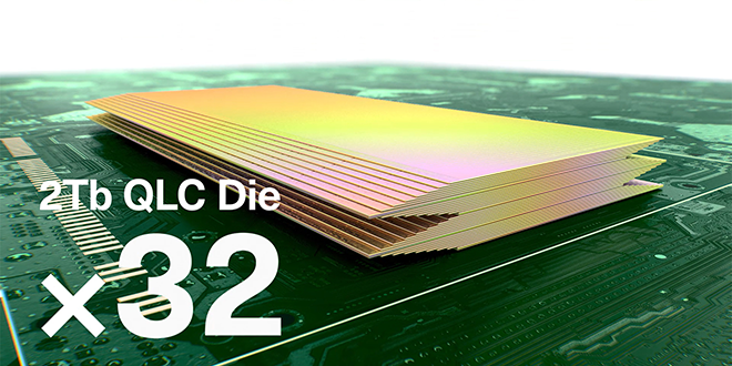
鎧俠透過在單一封裝內堆疊 32 顆容量各為 2Tb 的快閃記憶體晶粒,成功開發出大容量 8TB 快閃記憶體。這個記憶體解決方案得益於我們先進的後端製程技術,包括晶圓薄化、材料設計和打線接合技術。
專訪
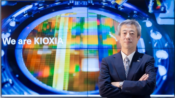
Leading the AI Evolution with Innovative 2mm Flash Memory Assembly Technology
32 memory dies assembled into a single package
The rapid growth of AI has accelerated demand for flash memory capacity. KIOXIA has successfully developed large-capacity 8 TB (terabyte) flash memory by assembling 32 pieces of 2 Tb (terabit) memory dies into a package less than 2 mm in height. This achievement was made possible with advanced assembly process technologies, including the technology for making wafers as thin as possible.
各世代共通的 BiCS FLASH™ 基礎技術
TLC (三層單元)和 QLC(四層單元)技術
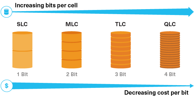
BiCS FLASH™ 3D 快閃記憶體產品線同時包含每單元 3 位元(TLC)與每單元 4 位元(QLC)技術。QLC 技術將每個記憶體單元的資料位元數從 3 位元提升至 4 位元,大幅提升了儲存容量。
利用 BiCS FLASH™ QLC 技術,在 16 層晶片堆疊架構下,單一封裝內即可實現高達 4TB 的容量。
鎧俠是業界首批預見並為儲存技術成功轉型做足準備的廠商之一,推動 SLC 到 MLC、從 MLC 到 TLC,以及從 TLC 到 QLC 的演進歷程。
鎧俠 QLC 技術是需要高密度、低成本儲存解決方案應用的理想選擇。現今的 QLC 技術,憑藉單一封裝所能實現的最高可用密度,有效縮減了空間占用,使儲存解決方案得以大規模擴展。

產品應用
無論是車用,輕巧高效能的個人電腦或是雲端伺服器以及超大規模資料中心部署,鎧俠記憶體和儲存解決方案透過提供先進的高效能、高密度、低功耗、低延遲、可靠性等功能,實現新興應用的成功,並讓現有技術發揮其可預期的潛力。
支援

如果您有任何技術疑問、想了解更多訊息、對樣品或採購商用產品(記憶體晶片、SSD)有興趣,請與我們聯繫。

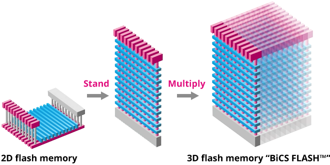
In 2007, KIOXIA announced the world‘s first 3D flash memory technology. Presenting our cutting-edge technologies, along with the key points of innovation and our efforts toward further increases in capacity.

KIOXIA invented the world’s first NAND flash memory in 1987. This is an explanation of the structure of flash memory and the mechanism of data storage.


